In this chapter we will discuss one of the most frequently use type of transducers: the strain gauge. A strain gauge is in fact nothing else than a resistor that changes its value as a result of a deformation. First, in Section 1.3.1 we will discuss what we exactly mean by ‘strain’. Next, in Section 1.3.2 we will start by discussing the most basic type of strain gauge: the metal strain gauges. In Section 1.3.3 we will continue with semiconductor strain gauges, which have a much higher sensitivity because the resistivity of the material itself is dependent on the strain. Finally, in Section 1.3.4 we conclude the chapter with an example of an accelerometer with strain gauge readout in which we will discuss the optimal placement of the strain gauges.
In this chapter a number of Greek symbols are frequently used:
![]() (sigma) - used to indicate stress
(sigma) - used to indicate stress
![]() (epsilon) - used to indicate strain
(epsilon) - used to indicate strain
![]() (nu) - used to indicate the Poisson ratio
(nu) - used to indicate the Poisson ratio
![]() (rho) - used to indicate the resistivity of a material
(rho) - used to indicate the resistivity of a material
![]() (pi) - piezoresistive coefficient: relative change in resistivity per unit stress
(pi) - piezoresistive coefficient: relative change in resistivity per unit stress
1.3.1. Metal strain gauges
The electrical resistance of a piece of metal like the beam shown in Figure 1.3.1 depends on its size and shape. For a rod with cross-section A and length L the resistance R is given by:
|
(1.41) |
with ρ the electrical resistivity or specific resistance of the metal. If as a consequence of an external load the resistor changes its dimensions the resistance will change. We can express the change in resistance dR as:
|
(1.42) |
If the rod is subject to an axial stress the change of the length and the change of the cross-section both lead to an increase (tensile stress) or a decrease (compressive stress) of the resistance.
The reason is that the changes of the length and of the cross-section have different signs. We have
|
(1.43) |
and
|
(1.44) |
Inserting (1.43) and (1.44) in (1.42) we find for the change of the resistance:
|
(1.45) |
And for the relative change:
|
(1.46) |
The ratio of the relative change of the resistance per unit strain is called the gauge factor G. Typical values of ν are between 0.1 and 0.4, so for most materials the gauge factor is between 1 and 2. The yield strain of metals, i.e. the strain level at which plastic deformation occurs, is mostly well below 1% (this is about the yield strain of high quality steel). Therefore, the resistance change of metal strain gauges is generally less than 1 or 2%.
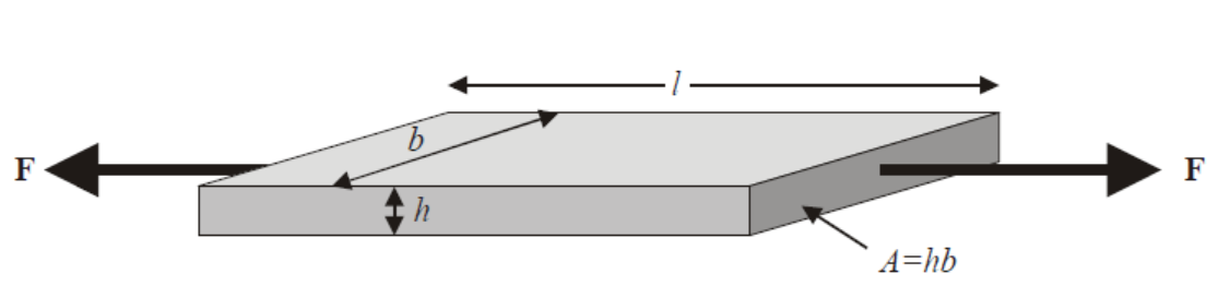
Figure 1.3.1: A beam subject to a tensile force
Metal strain gauges are developed to a very high level. On the market there are strain gauges of all possible kinds, including temperature compensated strain gauges and strain gauges that match a great number of materials. Figure 1.3.2 shows an example of metal strain gauges that can be glued to the structure of which the deformation should be measured. To give an indication what traditional technology after 100 - 200 years development and experience is able to: there are load cells based on metal strain gauges with a precision of 1:105, guaranteed in a temperature range between -40 and +80 oC. The load cell element for large loads (50 tons) can be made for a price of a few hundred dollars. Current micro technology cannot tip at this performance.
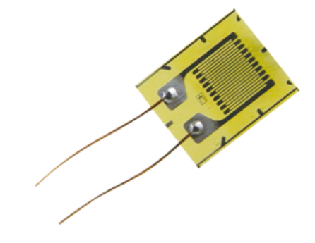
Figure 1.3.2: A typical metal film strain gauge (source: http://www.kyowa-ei.com).
1.3.2. Semiconductor strain gauges
The dominant effect in metal strain gauges is the change of the geometry. The materials property ρ is independent of the strain. This is different in semiconductors. The effect is called piezoresistivity and is present in materials like germanium, monocrystalline and polycrystalline silicon, amorphous silicon, and silicon carbide. Most common are silicon strain gauges. Silicon carbide strain gauges are mainly used in high-temperature applications (>600 oC) where silicon already starts to suffer from plastic deformation. In single crystalline silicon the effect is exploited by doping p-regions in n-type silicon microstructures. Polysilicon thin films can be deposited on top of microstructures, doped and pattered. Conductivity, and therefore all effects connected to conductivity such as piezoresistivity in crystals are anisotropic, i.e. dependent on the crystal direction. We do not dwell here into these complications, but refer to the literature; Kloek (1994) gives a good overview.
The piezoresistive coefficient π is defined as the relative change of the resistivity per unit stress, so that the change in resistivity can be expressed as
|
(1.47) |
There is a longitudinal and a transversal effect: the resistivity changes in a direction parallel to the strain and normal to the strain.
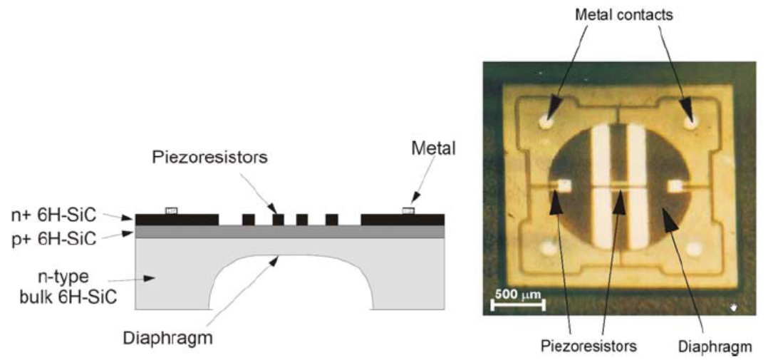
Figure 1.3.3: Cross-section and photograph of a pressure sensor chip with silicon carbide strain gauges realized in a thin layer on top of a flexible structure (source: http://www.kulite.com).
The piezoresistive effect in single crystalline silicon
The gauge factor in silicon depends on the crystallographic orientation and on the doping. The maxima of the coefficients are:
|
(1.48) |
The piezoresistive gauge factor can be found easily from π. If we include the change of the specific resistivity ρ in Eq. (1.46), we have
|
(1.49) |
The suffixes l and t refer to longitudinal and transversal piezoelectric coefficients.
The product of the piezoresistive coefficient π and the Young’s modulus of silicon is about 100, i.e. much larger than (1+2ν), so the geometric effect can be completely neglected, resulting in:
|
(1.50) |
Figure 1.3.4 shows a cross section of a typical silicon pressure sensor using integrated monocrystalline silicon strain gauges to measure the bending of a membrane that deforms under a pressure difference. The strain gauges are p-type diffusions in an n-type silicon layer that is epitaxially grown on a p-type silicon substrate. In this way the n-type silicon layer can be used as an etch-stop when etching the membrane. An important advantage of silicon pressure sensors is that the electronics can be integrated on the sensor chip. Figure 1.3.5 shows some examples of pressure sensors combined with NMOS and CMOS electronics.
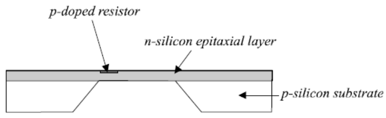
Figure 1.3.4: Pressure sensor configuration with p-type piezoresistors integrated in an n-type epitaxial layer. The epitaxial layer is also used as etch stop for realizing the membrane.
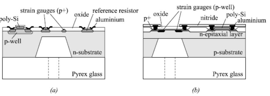
Figure 1.3.5: Two examples of piezoresistive pressure sensors with monocrystalline strain gauges and integrated electronics: (a) an NMOS process (Tanigawa 1985), and (b) a CMOS process (Kress 1991).
The first silicon pressure sensors were based on a piezoresistive read-out mechanism, and, at the moment, piezoresistive pressure sensors are still the most widely used. The piezoresistors may be diffused in the membrane as in Figure 1.3.4 or deposited on top of the membrane. The latter involves a much more complicated fabrication process: an isolation layer (usually silicon dioxide) is deposited on the sensor wafer and then another silicon wafer containing the strain gauges is fusion bonded to the isolation layer. Figure 1.3.6 shows an example of such a sensor. The main advantage of the bonded strain gauges is the good electrical isolation of the silicon dioxide layer. Standard diffused strain gauges suffer from leakage currents through the pn junctions, especially at higher temperatures.
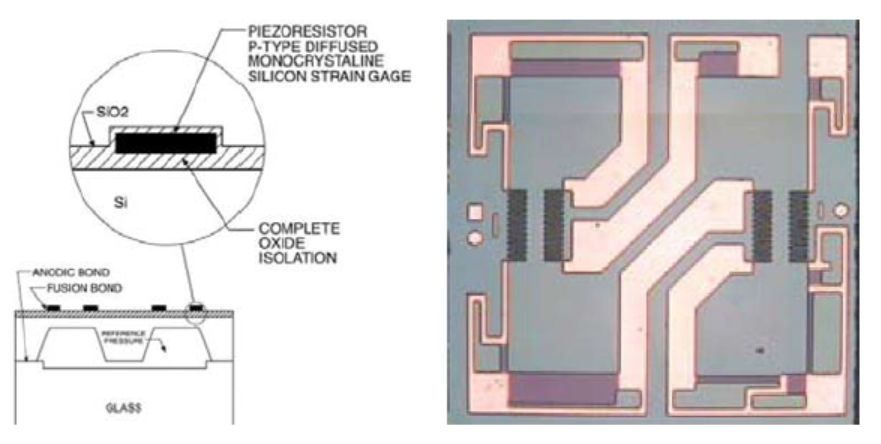
Figure 1.3.6: Cross-section and photograph of a pressure sensor chip with monocrystalline silicon strain gauges realized in a thin layer on top of a flexible structure (source: http://www.kulite.com).
As a final example, Figure 1.3.7 shows a cross section of an accelerometer with piezoresistive strain gauges to detect the displacement of the proof mass. It consists of a central silicon wafer containing the proof mass and a cantilever suspension beam. The wafer is bonded between two glass wafers to protect the structure and provide shock stop and damping. A piezoresistor is integrated in the suspension beam. When the proof mass moves with respect to the support frame the suspension beam bends, resulting in a change in resistance of the piezoresistor.
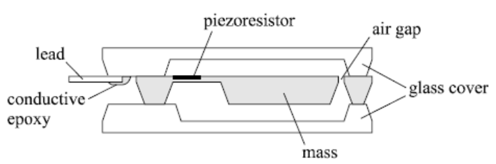
Figure 1.3.7: Structure of a piezoresistive accelerometer (Roylance 1979).
The piezoresistive effect in polysilicon thin films
Polysilicon thin films deposited by low-pressure chemical vapour deposition (LPCVD) processes on top of flexible structures can also be used as piezoresistive strain gauges. They have a few advantages compared to indiffused or implanted resistors: the technological possibilities allow a greater freedom of design and the choice of materials for membranes is greater, and the strain gauges do not rely on junction isolation, so there are less problems with leakage currents and larger voltages can be used. Electrical isolation from the substrate is done by means of a dielectric thin film as show in Figure 1.3.8 (preferably stress free silicon nitride). Electrical contact can be made either by highly-doped polysilicon leads, or better, because of higher conductivity, by metal leads.
Similar to single crystalline silicon, the piezoelectric coefficient in p-doped silicon is larger than in n-doped silicon. Using polysilicon it is possible to realize films with both types of doping, in contrast to implanted strain gauges. However, due to grain boundary effects and texture, the size of the piezoresistive effect is reduced. The maximum gauge factor in p-doped polysilicon is close to -40, in n-doped polysilicon to +20.
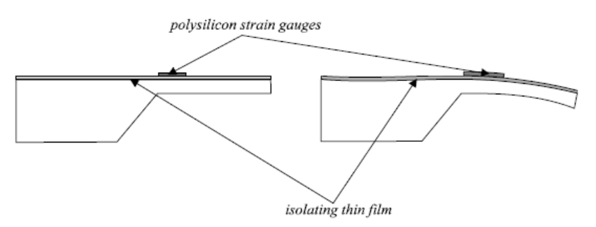
Figure 1.3.8: Polysilicon strain gauges realized in a thin layer on top of a flexible structure.
Important work on piezoresistive pressure sensors using surface micromachined polysilicon membranes has been done by Guckel. Figure 1.3.9 shows a schematic drawing of a typical device (Guckel 1993). An SiO2 layer is used as the sacrificial layer. The polysilicon membrane is about 2 μm thick and is deposited using low-pressure chemical vapor deposition (LPCVD). Deposition of a polysilicon layer with reproducible mechanical properties is not easy, as the mechanical properties of polysilicon are related to the film morphology and LPCVD polysilicon can have a wide morphological range. Furthermore, the built-in strain has to be controlled carefully, as a compressive strain may cause buckling of the membrane and a large tensile strain reduces the sensitivity. Therefore, after deposition an anneal step is used to convert the initially compressive strain into a tensile strain.
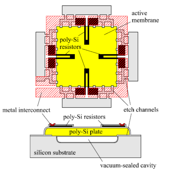
Figure 1.3.9: Surface micromachined pressure sensor with polysilicon membrane (Guckel 1993)
1.3.4. Optimal placement of the strain gauges
In the examples given so far you may have noticed that the strain gauges are always located at the edge or in the center of a deforming structure. This is no coincidence! In Chapter 1.2 we have already seen that in the example of a cantilever beam the maximum strain occurs at the fixed side at x=0. This is the position where the internal bending moment is the largest, and thus the curvature and the strain at the surface are also the largest. In this section we will look at two frequently occurring situations: a cantilever beam loaded by a force at the end, and a beam that is fixed at both ends (a so-called clamped-clamped beam) and loaded by a force in the center. Finally, we will discuss an accelerometer structure based on a clamped-clamped beam configuration.
A cantilever beam loaded by a force at the end
For the case of a cantilever beam with length L, width b and height h, fixed at one end and loaded by a force F at the other end we already found an expression for the deflection in Chapter 1.2, equation (1.34):
|
(1.51) |
Where I is the second moment of area of the beam:
|
(1.52) |
We also found that the strain increases with the distance from the neutral line and is the highest at the surface. For a cantilever beam with height h, the distance of the surface from the neutral line is h/2, and we find the strain from equation (1.28):
|
(1.53) |
Inserting (1.51) into (1.53) we find for the strain at the surface of the beam:
|
(1.54) |
We now immediately see that the strain changes linear with x and has a maximum ![]() at x=0 and a minimum equal to zero at x=L. The latter we could also have deduced from the fact that there is no moment acting on the end of the beam so there will be no curvature at the end of the beam.
at x=0 and a minimum equal to zero at x=L. The latter we could also have deduced from the fact that there is no moment acting on the end of the beam so there will be no curvature at the end of the beam.
For optimal sensitivity the strain gauges should be located near the beginning of the beam. For strain gauges with a length l, the measured average strain is:
|
(1.55) |
So we see that the measured strain decreases with an increase in length of the strain gauges and, therefore, it is usually preferred to have a meandering strain gauge near the beginning (x=0) of the beam instead of having a strain gauge over the entire length L of the beam.
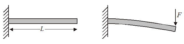
Figure 1.3.10: Cantilever beam with point force F at the end of the beam
A clamped-clamped beam loaded by a force in the center
Figure 1.3.11 shows a clamped-clamped beam configuration loaded by a point force in the center. In this case the deflection w as a function of the position x along the beam is given by:
|
(1.56) |
A good exercise would be to derive (1.56) yourself with what you have learned in the previous chapter!
The largest deflection now occurs in the middle of the beam at x=L/2:
|
(1.57) |
inserting (1.52) for the second moment of area.
The strain is now given by:
|
(1.58) |
Thus the strain changes again linear with x and has maxima ![]() and
and ![]() at x=0 and x=L/2, respectively. Thus, for optimal sensitivity the strain gauges should now be located near the ends (tensile strain) or near the center (compressive strain) of the beam. We can again calculate the average strain that is measured by strain gauges with a length l:
at x=0 and x=L/2, respectively. Thus, for optimal sensitivity the strain gauges should now be located near the ends (tensile strain) or near the center (compressive strain) of the beam. We can again calculate the average strain that is measured by strain gauges with a length l:
|
(1.59) |
So we see that the measured strain decreases with an increase in length of the strain gauges similar to the case of a cantilever beam, but now the average strain may even become equal to zero if l is equal to L/2. A strain gauge across the entire beam will measure nothing!
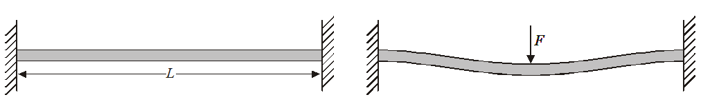
Figure 1.3.11: Clamped-clamped beam with point force F at the center of the beam
Example: an accelerometer with strain gauge readout
We can easily realize an accelerometer based on a clamped-clamped beam configuration: we just need to insert a proof mass in the center of the beam. Equation (1.57) then gives the displacement of the proof mass. The spring constant K is given by:
|
(1.60) |
resulting in a resonance frequency equal to:
|
(1.61) |
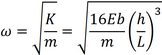
The displacement of the proof mass due to a static acceleration a is given by:
|
(1.62) |
The resulting strain measured by the strain gauges can be calculated directly from (1.58) and (1.59).
Of course, depending on the suspension and how the mass is attached to it, the sensor may be sensitive to acceleration and rotation in various directions. In fact, this can be exploited to realize an accelerometer that measures acceleration in multiple directions using a single proof mass. Figure 1.3.12 shows an example of such a sensor: an accelerometer that measures the three components of linear acceleration plus rotational accelerations around three orthogonal axis using 20 piezoresistive strain gauges.
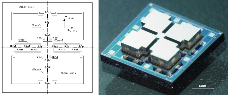
Figure 1.3.12: Strain gauge layout and photograph of a six-degree-of-freedom piezoresistive accelerometer (Amarasinghe, 2005).
1.3.5. References
Amarasinghe R., Dao D.V., Toriyama T. and Sugiyama S., "Design and fabrication of a miniaturized six-degree-of-freedom piezoresistive accelerometer," J. Micromech. Microeng. 15, 2005, pp. 1745–1753.
Guckel H., “Surface micromachined physical sensors,” Sensors and Materials, 4, 1993, pp. 251-264.
Kloek B., “Piezoresistive sensors,” in Sensors, Vol. 7, ed. W. Göpel, J. Hesse and J.N. Zemel, VHC Verlagsgesellschaft, Weinheim, Germany, 1994, pp. 145-172.
Kress H.-J., Bantien F., Marek J., Willmann M., “Silicon pressure sensor with integrated CMOS signal-conditioning circuit and compensation of temperature coefficient,” Sensors and Actuators A, 25-27, 1991, pp. 21-26.
Roylance L.M., Angell J.B., “A batch fabricated silicon accelerometer,” IEEE Trans. Electron. Devices, ED-26, 1979, pp. 1911-1917.
Tanigawa H., Ishihara T., Hirata M., Suzuki K., “MOS integrated silicon pressure sensor,” IEEE Trans. Electron Devices, ED-32, no. 7, 1985, pp. 1191-1195.